
STMicroFlowA
Documentation for ST Micro 0.13u design flow
Licenses needed for the design flow
- Cadence Virtuoso
- Calibre DRC/LVS
- Calibre Connectivity Interface (CCI)
- Star RCXT
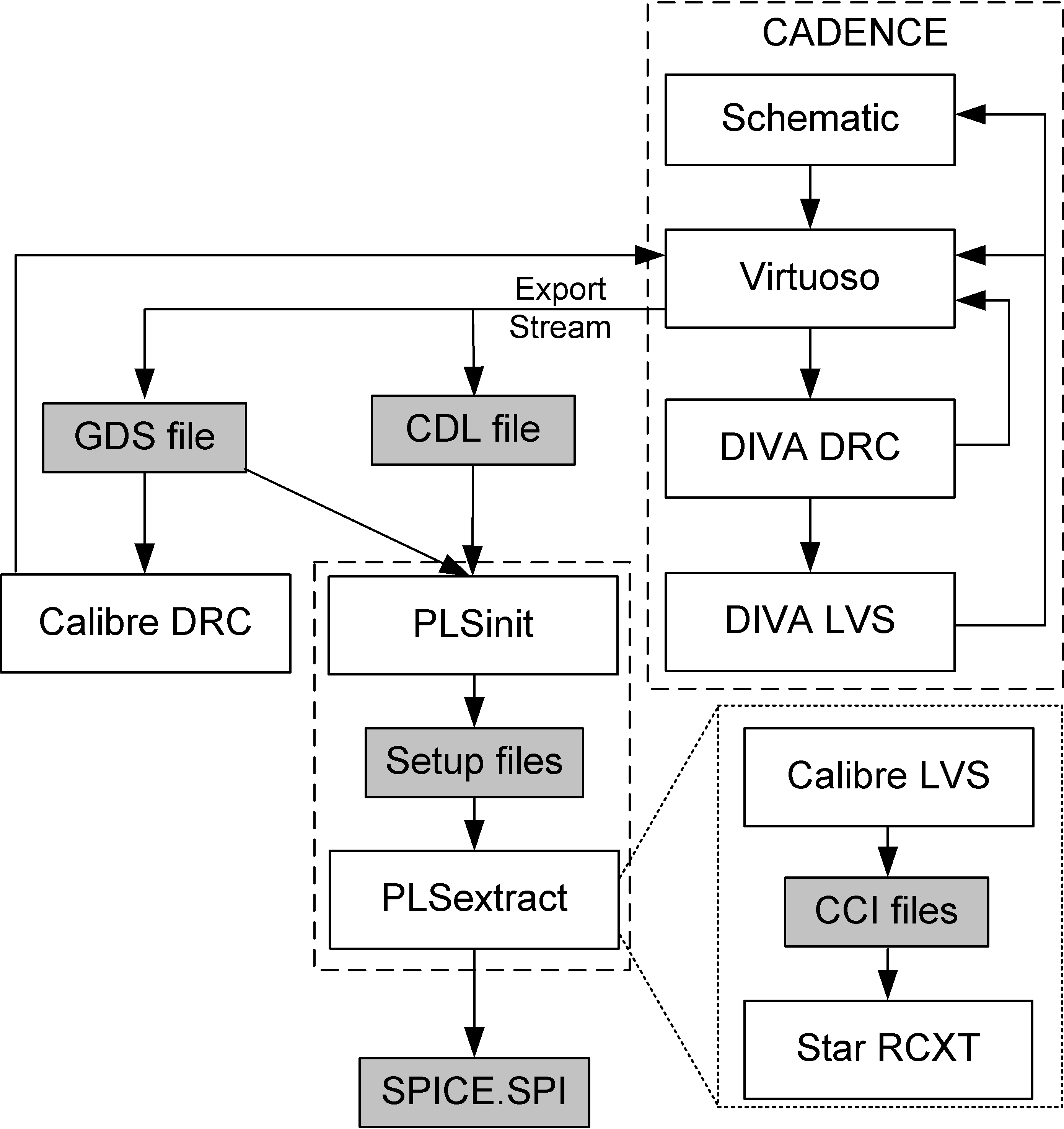
ST Micro 0.13u Design Flow Scheme
General Design Tips
- Make sure that all projects use unique Library names (also use unique names for decaps and fill-metal cells) to avoid name conflicts during assembly.
- Flooplan of the chip should be decided as early as possible during the design flaw. This reduces the final assembly time considerably.
- Each project should have schematic of top cell so that LVS of the entire (assembled)chip could be run.
- Do not use 45 degree angles for paths, because it may cause off-grid errors. If necessary, use 45 degree angles only for polygons.
- Instead of fingering transistors place several transistors in parallel because DivaLVS does not support fingered transistors
Note
When making layout in Virtuoso Layout editor, in order to make extraction tools and Calibre LVS working the nets to which the pins will be attached must be labeled. One simple way to do this is as follows:
1.First label the appropriate nets, (select pintext for appropriate layer eg. metal1 pintext, poly pintext etc.)
2.then in Virtuoso Layout editor choose Create/Pins From Labels to create the pins.
General Setup
Before starting the design first make sure that the module stm/cmos9gp/8.2.1 is added by typing:
module list
If the module is not added you should add it by typing:
module add hcmos9gp-9.2
This will load all the modules needed to run the ST CMOS9GB flow. To start a new design you need to setup your environment like the following:
      mkdir <dirname>
      cd <dirname>
      cp /chalmers/sw/sup/cds/hcmos9gp-9.2/install/setup_working_dir/.cdsinit .
      cp /chalmers/sw/sup/cds/hcmos9gp-9.2/install/setup_working_dir/.simrc .
      cp /chalmers/sw/sup/cds/hcmos9gp-9.2/install/setup_working_dir/.ucdprod .
      cp /chalmers/sw/sup/cds/hcmos9gp-9.2/install/setup_working_dir/cds.lib .
Start Cadence by typing:
> icfb &
Alternately, the command stm_130 carries out these steps for you once you have changed into the directory of your choice. It also starts up the correct Virtuoso version required.
Setup for Spectre simulation
Start the Affirma Analog Circuit Design Environment (henceforth called AACDE). Choose Setup -> Model Libraries. You'll get a Model Library Setup dialog. In the text field at the bottom of the dialog, enter the library name of the five-corners MOS parameter library:
/cab/ce/sw/foundry/stm/hcmos9gp/8.2.1/DK_hcmos9gp_A_M6_3V3_HSLL_8.2.1/MODULES/DKhcmos9gp_A_M6_3V3_HSLL_spectre/CORNERS/mosfet.scs
In the Section field at bottom right, enter
TT
or, for that matter,
FF, SS, SF or FS.
Click on Add. The library definition shows up in the panel above the field you just entered it into. Click OK. Netlist and run in AACDE as usual.
DRC and LVS
All paths begin with:
/cab/ce/sw/foundry/stm/hcmos9gp/8.2.1/DK_hcmos9gp_A_M6_3V3_HSLL_8.2.1
The rule files needed for DRC and LVS with DIVA can be found at:
      ./MODULES/DKhcmos9gp_M6_OpusTechfile/DK_hcmos9gp_M6/divaDRCEXT.rul
      ./MODULES/DKhcmos9gp_M6_OpusTechfile/DK_hcmos9gp_M6/divaLVS.rul
The rule files for DRC and LVS with Calibre can be found at:
      ./MODULES/DKhcmos9gp_M6_3V3_HSLL_calibre/hcmos9_6ML_HS_noUHS_LL_noULL_3V3.calibredrc_cgi
      ./MODULES/DKhcmos9gp_M6_3V3_HSLL_calibre//hcmos9_6ML_HS_noUHS_LL_noULL_3V3.calibrelvs_cgi
The tool to be used for DRC and LVS during the early stages of the layout of a cell is DIVA. DIVA is a simple tools and not all design rules are in the DIVA rule files. DIVA is however integrated into the Cadence tools which makes it convenient to use early in the design phase to catch most of the DRC errors. There is a possibility to convert the rule files for DIVA so that they can be used together with Assura which is a newer and more competent tool. There would of course still be missing design rules but the tool might be easier to work with.
Calibre is the tool to be used for final sign off and has a complete set of design rules including coverage. To run calibre load the module and then start it by typing:
calibre -gui
To run Calibre DRC you first have to stream out a GDS file for the layout to be checked. To stream out the GDS file, in Cadence icfb window choose File/Export/Stream... . In the Stream Out window press Library Browser to select the layout view of the circuit from which the GDS file will be extracted and press OK.
DRC Rules
| Rule | Value |
| METAL Coverage | 20% to 80% |
| Poly Coverage | 14% |
| Active density | 16% |
| NPLUS PPLUS enclosure of poly | >=0.20um |
| AluCap density (Use MIM layer) | 12% |
Parasitic Extraction
Read the Note message in General Design Tips section!
Extraction of parasitics is done using the Post Layout Simulation (PLS) extraction tool (interface) provided by foundry. PLS extraction interface employs two tools to execute the extraction: Calibre LVS (to generate the Calibre Connectivity Interface (CCI) files) and Star-RCXT (to do the extraction). PLS interface generates setup files for Calibre LVS and Star-RCXT and runs these tools automatically. PLS needs only GDS and CDL (circuit description language) files to do the extraction. To extract the CDL file in Cadence icfb window choose File/Export/CDL.... In the CDL Out window press Library Browser to select the schematic view of the circuit from which the CDL file will be extracted and press _OK_. PLS is executed in two steps as follows: 1.To start the initialization of the extraction flow, type:
PLSinit -gui
In Edit PLSinit parameters window indicate the paths to the GDS and CDL files (and cell names) and choose netfile location: Generate netfile with all nets . Let the remaining options be default. 2. To start the extraction, type:
PLSextract -gui
The output of the extraction flow is SPICE.SPI file.
Alternately, a plugin provided by ST Micro enables PLS from the layout window. It can be found under Tools --> *Post-Layout Simulation --> Textual Netlist Import
Running this command brings up a GUI where many of the options mentioned above are automatically done. However, the modules for StarRCXT and Calibre must be added if you have not done so (using module add hcmos9gp-9.2 adds all of the tools required; so it is recommended that this module be used.)
Debugging the extraction flow
If PLS extraction is failing you should check if Calibre LVS can run separately without errors with the setup files generated by PLSinit. PLSinit creates two directories: extractRunDir and initDir. initDir contains the setup files required for PLSextract, whereas extractRunDir is empty. extractRunDir will contain Run directories (LvsRunDir and RCextract) in which Calibre LVS and Star-RCXT will automatically be executed. When started, PLSextract creates those Run directories, copies into them the necessary setup files from initDir (also generates some additional ones) and executes Calibre LVS and Star-RCXT.
Go to extractRunDir/LvsRunDir (if you have started PLSextract the LvsRunDir and RCextract directories with the setup files inside them should already be created). To start Calibre LVS GUI with required setup, type:
calibre -gui -lvs calibreGuirunsetlvs -custom calibreGuiswitchdef
and press OK in Customization Settings window, then press Run LVS in Calibre Interactive window. When LVS is finished, press Start RVE in Calibre Interactive window to see the result. In RVE window it should state: "LVS Results: Designs Match". Ignore the warning message: "WARNING: Cannot enable LVS PUSH DEVICES because pin location information was requested" in the Extraction Report window.
If designs are not matching one way to look for errors is to compare the schematic and layout netlists visually. In RVE window press on Source netlist and Layout netlist to monitor schematic and layout netlist, respectively. The potential cause of mismatch can be that in the layout design some of the nodes (wires) that are connected to the pins are not labeled and therefore those pins (terminals) are not present in the subcircuit definition when layout netlist is created. Hence, one should check if subcircuits in schematic and layout netlists have the same (number of) pins (terminals).
Chip Assembly Tips
    * The right places to get VDD for circuit's core are:
      main: metal2 pins on VDDCO_65 or on VDDIOCO_65 pad
      other: internal ring of metal6 in IO ring.
      The right places to get VSS (ground) for circuit's core are:
      main: metal2 pins on VSSCO_65 or on VSSIOCO_65
      other: internal ring of metal5 in IO ring.
      This information was provided by CMP

      The right places to get VSS (ground) for circuit's buffers are:
      main: metal2 pins on VSSIO_65 pad
      other: gnde ring in metal3 in IO ring (use metal1 wires and M3_M1 vias to reach it)
      The right places to get VDD (ground) for circuit's buffers are:
      main: metal2 pins on VDDIO_65 pad
      other: vdde ring in metal3 in IO ring (use metal1 wires and M3_M1 vias to reach it)
      This is is how we did in our first chip
For the sake of simplicity in our chips it should be possible to use VDDCO_65 pad for core VDD, VDDIOCO_65 pad (and internal ring of metal6 in IO ring) for buffer VDD and VSSIOCO_65 pad (and internal ring of metal5 in IO ring) for core and buffer ground
- Note, that usage of VDDIOCO_65, VSSIOCO_65, VDDIO_65 and VSSIO_65 pads is mandatory
- Use ANA_65 pad for inputs and outputs
- Minimum distance between the pads in the pad ring is 5um. If you place 18 IOFILLER2_65 cells (from library IOLIB_65_M6_LL) between the pads the distance between the pads will be 5.14 um (which is quit close to min distance). One can use other combinations of IOFILLER2_65, IOFILLER3_65, IOFILLER4_65, IOFILLER8_65, IOFILLER16_65, IOFILLER32_65, IOFILLER62_65 and IOFILLER64_65 cells to create the pad ring (and IO ring). It is handy to create your own block (cell) of filler cells that gives min distance between the pads and use it to create a pad ring (and IO ring).
- IOLIB_65_M6_LL library cells have reduced layout i.e. layout contains only metal layers and vias but no transistors. These library cells will be replaced with full layout versions by CMP when design is submited. Note, that IO ring sections of the pad cells must overlap with filler cells by 0.11um in order to avoid DRC errors that otherwise will occur when IOLIB_65_M6_LL library cells will be replaced with full layout versions.
- Use LTCORNER_65, LBCORNER_65, RTCORNER_65, RBCORNER_65 cells from IOLIB_65_M6_LL library to fill the left top, left bottom, right top and right bottom corner of the chip, respectively.
- Minimum distance between the IO ring and probing pads placed in the middle of the IO ring is 108.1550um
- Before running Calibre DRC in the Customization Settings window select ClassF1
Things To Be Done
- Check if automatic filling of metal is available
- Investigate how to run Spectre simulations with SPICE.SP file
- Check how to run Calibre DRC and parasitic extraction from Cadence environment